Blackwell architecture and distributed AI training scale
Nvidia Blackwell architecture delivers a 30x performance increase for LLM inference workloads compared to the H100 GPU. The new silicon features 208 billion transistors and utilizes liquid cooling to manage thermal design power reaching up to 1,200W.

High performance through Blackwell silicon
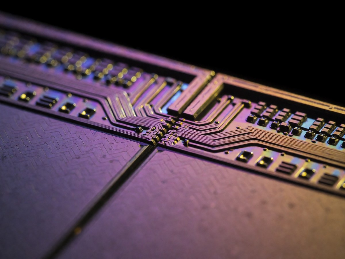
Nvidia Blackwell architecture replaces the Hopper series to power real-time generative AI on trillion-parameter large language models. The Blackwell GPU contains 208 billion transistors, which doubles the 80 billion transistors in the Hopper series. The GB200 Superchip connects two B200 GPUs and an Nvidia Grace CPU over a 900GBps chip-to-chip link and provides a 30x performance increase for LLM inference workloads compared to the Nvidia H100 GPU. This architecture reduces cost and energy consumption by up to 25x compared to the predecessor Hopper series. TSMC manufactures Blackwell architecture GPUs using a custom-built, two-reticle limit 4NP process with GPU dies that connect via a 10TBps chip-to-chip link into a single, unified GPU. The hardware includes a second-generation transformer engine and new 4-bit floating point AI inference capabilities. It also contains a dedicated engine for reliability, availability, serviceability, and maintenance to run diagnostics and forecast reliability issues. The architecture includes a dedicated decompression engine to accelerate database queries. David Harold Blackwell, a mathematician who specialized in game theory and statistics, provides the namesake for this architecture. Amazon, Google, Meta, Microsoft, Oracle Cloud, and OpenAI will deploy Blackwell GPUs later this year. You should recognize that these major players define the trajectory for massive model training.
| GPU Architecture | Thermal Design Power | Interconnect Generation |
|---|---|---|
| Hopper | Up to 700W | NVLink 4.0 |
| Blackwell | 700W to 1,200W | NVLink 5.0 |
| Rubin | 1,800W | NVLink 6.0 |
| Feynman | 4,400W | Immersion Cooling |
Scaling communication via NVLink
Scaling large language models requires high-speed interconnects that bypass the PCIe bus bottleneck. NVLink 5.0 delivers 1,800 GB/s per GPU and uses 200 GT/s PAM4 signaling. Within an NVL72 rack, nine NVSwitch trays provide 130 TB/s of aggregate bandwidth. Every GPU in the NVL72 domain can access the memory of every other GPU at line rate without contention. NVSwitch chips in the Blackwell era provide 72 ports per chip, and this provides enough capacity to wire 72 GPUs all-to-all at full radix through a copper-cable backplane. For a 1T-parameter model stored at 16-bit precision, the training process requires 2 TB of parameter storage. A training run using the Adam optimizer requires memory peaks roughly seven times the model parameter size in intermediate memory. The network requirements for training these models change significantly as parameter counts grow. For large-scale distributed training, engineers use 100 to 400 Gbps interconnects and rely on RDMA to reduce latency and improve throughput. A 200 Gbps network port cannot be fully utilized when attached to a PCIe 3.0 x16 host bus because that bus provides only 16 GB/s per direction. If packet loss reaches 1%, the GPU compute-time fraction falls by 13%. If dynamic latency increases from 10 microseconds to 1000 microseconds, the GPU compute-time fraction drops by nearly 10%. Moving from a single NVLink domain to 576 GPUs across multiple racks requires InfiniBand, which operates at 30x slower speeds than NVLink. Does the transition to InfiniBand create an insurmountable latency gap for tensor-parallel workloads?
Thermal management for high power density
Increasing compute density forces a shift toward liquid cooling solutions. Blackwell GPUs operate between 700W and 1,200W depending on the SKU and cooling type. Because Blackwell increases heat dissipation to 1,200W, liquid cooling becomes mandatory. Future architectures like Rubin will increase thermal design power to 1,800W, while Feynman reaches 4,400W. Feynman Ultra will increase TDP to 6,000W. Researchers at KAIST predict the TDP of AI GPUs will increase to 15,360W by 2035. These extreme thermals require the use of immersion cooling where entire GPU-HBM modules sit in a thermal fluid. Immersion cooling should satisfy thermal needs until 2032, when post-Feynman GPU architectures increase per-package TDP to 5,920W or 9,000W for the Ultra variant. The industry will use direct-to-chip liquid cooling for Rubin Ultra. Post-Feynman models will see power consumption for memory reach 2,000W because each of the 16 HBM stacks reaches 120W. These processors will use thermal vias (TTVs) and fluidic TSVs (F-TSVs) to manage heat. By 2038, manufacturers will use double-sided interposers and GPU-on-top architectures to prioritize heat removal.

Technewsdaily
Senior tech writer covering AI, gadgets and cybersecurity. Breaking down the news that matters, every day.